Nanoelectronics is one of the key enabling technologies to open up new paths for inventing new products and processes and advancing current technology. Potential for Germany as a location for suppliers and manufacturers in nanoelectronics is seen especially in exploiting emerging technology paths in which the current technological position as well as framework conditions for valorisation are considered to be more favourable than in the current miniaturisation path. The aim of this study is firstly to identify those technological developments and applications that are important for commercialisation (e.g., high market potential). Secondly, development paths together with related barriers are identified as a basis for a strategic approach to exploit the potential of these developments.
Nanoelectronics – Emerging Economies Competing with High-tech Countries
Micro-/nanoelectronics has been in the focus of the strategic policies of various countries for decades now. Industrialised and especially emerging countries expect high impact on growth and on highly skilled employment in related high-tech industries. Significant changes can truly be seen in the geographic distribution of this industry and related markets within the last decade:
- After tremendous shifts in the last two decades, the Asian countries dominate the demand for nanoelectronic products with a combined market share of about 70%. In contrast, Europe only accounts for 13% of the worldwide demand.
- In Europe, the share of worldscale production capacity has decreased between 2000 and 2009 from 15% to below 10%. Germany as the largest producer in Europe has also lost ground.
- In R & D-intensive chip design, American sites are still leading, but indvidual Asian countries (especially Taiwan) are catching up. European companies are focusing mainly on chip design for automotive and industrial electronics.
These changes cannot be explained by the catch-up strategies of emerging countries only. Fierce international competition is ongoing even at the technological frontier. To remain competitive, European countries, such as Germany, have to keep pace with the leading edge of technological development. But strategic advice on how to accomplish this cannot be given easily. Nanoelectronics is neither a clearly defined technology, nor is its future development evolutionary and foreseeable as in the past when it consistently followed a dominant technological trajectory (the Moore’s law) for decades. Instead, nanoelectronics is usually broadly defined and includes all areas of electronics in which fine structures at the level of nanometres are used. Besides developments that simply downscale design principles known from microelectronics up to nanoscale (“More-Moore” path), other technological paths have recently received higher attention.
The “More-than-Moore” path is concerned with the extension of functionalities, while the “beyond CMOS” path addresses radical new components besides the traditional CMOS (complementary metal-oxide semiconductor) technology, which is the semiconductor technology used in the transistors that are manufactured into most of today’s microchips. Especially in the new technology paths, the knowledge base in Germany is often rated as highly competitive (e.g., Thielmann et al. 2009). However, it remains unclear which developments and applications are the most favourable to exploit and should be in the focus of R&D- and commercialisation activities. Hence, the current study aims to identify key emerging technology paths in which Germany can take an internationally leading position. In addition, it reveals related development paths and key barriers to enable and foster a transparent discussion on the development of a strategic approach. The study concentrates on a short (< 4 years) and a mid- to long-term outlook (> 8 years).
Combining Online Survey with Roadmapping
In order to reach the various aims of the study, we used a mix of methods resulting in two major steps. First, an online survey was conducted in order to identify those technological developments and applications important for commercialisation in Germany (defined by assumed market potential). Second, a technology roadmap was elaborated that allows the formulation of development paths and barriers. These methods are described below in more detail. Both steps were conducted by the project group as a whole with Fraunhofer ISI as the responsible partner for these two work packages. The work of the project group was accompanied by a steering group, which consisted of experts from academia and industry in the field of nanoelectronics in order to assure high quality standards.
Online Survey
The questionnaire for the online survey consisted of three major parts. First, an overall assessment of the relevance of the main technology trends (“More-Moore etc.) was requested. The second part contained three sub-parts and asked which materials and production processes, system components, and fields of application will become relevant in which time period (<3 years; 3-8 years: >8 years) and what their functional advantages will be (e.g., miniaturisation, reduction of production costs etc.). The third part consisted of statements for key technological developments and innovation barriers. These statements were based on expert interviews as well as on knowledge from earlier projects. They were discussed and re-formulated at a meeting with the steering group.
The questionnaire was online between early July and early October 2010. Two approaches were used in selecting the sample for the survey. First, experts of the steering group compiled a list of experts and contacted them by e-mail. Second, these experts were requested to forward the e-mail to other experts (snowball system). In total, 90 experts answered the questionnaire; the return rate of the experts directly contacted amounted to 37 %. About one half of the respondents were from academia and the other half from industry (mostly big companies). About two thirds of the respondents were closely related to the electronics sector; the other third was affiliated with a wide range of other areas (e.g., automotive industry, medical technology). While we cannot rule out in principle that the sample might lead to some biased results, we could identify neither any major differences in the answers between the respondents nor any other indications of underlying biases.
Roadmap
The task of the roadmap was to display the development paths over time, thus visualising the time sequence of the single steps of knowledge and technology development. For this purpose, we conducted an expert workshop with experts from academia and industry from different sectors in October 2010. The results of the second part of the online questionnaire (market relevance assessment of materials, production processes and system components) provided the main basis for the workshop. The aim was to formulate the development paths leading up to today’s market potential. Combining the results of the online-survey with the roadmap workshop allowed us to start the workshop from an advanced level of analysis and thus to describe and discuss the development paths in more detail.
In contrast to existing roadmaps (above all the International Technology Roadmap for Semiconductors – ITRS), we placed the regional focus on Germany combined with a high level of detail. However, the high awareness of the ITRS among the participants became evident during the roadmap workshop. Keeping the experts’ minds open to other developments posed a considerable challenge.
Sectors Absorbing Nanoelectronics
At the start of the survey, the participants were asked to rank the following six technological sectors in the order of importance for the German electronics industry:
- scaled microelectronics (“More-Moore”)
- functional diversification (“More-than-Moore”)
- new building blocks (“beyond CMOS”)
- packaging of integrated circuits
- testing and test equipment
- production lines
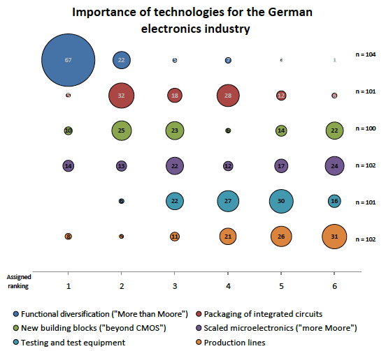
Among the sectors listed, “More-than-Moore”-technologies were ranked in the first position. Two thirds of the respondents voted them as of highest importance for the German electronics industry. A clear position was also taken in case of “production lines”, which were ranked in last place. “Testing and test equipment” was judged a little bit more important and placed in second to last place. All other technological sectors were judged ambiguously. This becomes especially obvious for “beyond CMOS” technologies, which seem to divide the respondents into two groups. However, a cross-analysis of the votes by professional background of the respondents failed to show any underlying pattern.
In the main part of the questionnaire, participants could choose between three areas of interest in which more detailed questions were posed: materials and production technologies, system components, and applications. In the part containing questions on system components, three of the previously listed technological sectors again were the subject of a single question. We were interested in the relevance of system components for the realisation of nanoelectronics’ worldwide market potential. The ranking under this aspect was different from the initial ranking. The answers were nonetheless quite comparable and unambiguous. “CMOS” technologies (“More-Moore”) was voted as of highest relevance, “packaging technologies” also as of high relevance, but “beyond-CMOS” only of moderate relevance. One can say that the group of experts who chose to answer here displayed a quite uniform opinion compared with all the respondents who ranked the six technological sectors at the beginning.
In order to identify the notably relevant topics from the entire collection of topics listed, we chose a special kind of technique for interpreting the responses. At earlier workshops, we could observe a typical behaviour among participants to rate those aspects as important that are expected to be available in the near future. Therefore we used a filter in order to identify important aspects while offsetting this effect. We looked for aspects that were judged as relevant even though they were not expected to become available anytime soon.
Sorted in the order of estimated availability, we could identify the following materials and production processes as of particular relevance:
- double patterning
- atomic layer deposition (ALD)
- organic semiconductors
- EUV-lithography
- carbon based materials
The following system components could be identified as of particular relevance:
- CMOS (evolutionary development)
- auto-diagnosis
- through-silicon via 3D integration
- nanoelectronic and optoelectronic mechanical systems
- auto-correction
- piezoresistive sensors
Nanoelectronics Applications
The relevance of nanoelectronics for certain industrial sectors and some exemplary applications was the subject of the third sub-part. For the industrial sectors, the relevance was stated as high or very high by at least 50% of all respondents. Nanoelectronics is considered of high importance especially for the sectors electronics, automotive/aeronautics and medical technologies.
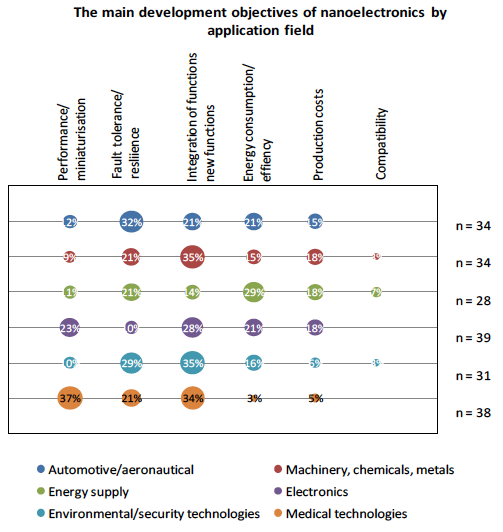
Investigating preferable development objectives for the individual sectors of application yielded further interesting results: The selected objectives differ considerably between the fields of application. For machinery/chemicals/metals, electronics and environmental/security technologies, integration of functions or new functions are of main importance. In contrast, the emphasis is on fault tolerance as the main objective for the automotive/aeronautical sector while for energy supply the issue of energy consumption/efficiency of course comes out on top. Interestingly, for medical technologies performance/miniaturisation and (integration of) new functions are ranked higher than fault tolerance/resilience, which is probably considered a precondition rather than a developmental goal for nanoelectronics.
Roadmap Workshop
The primary objective of the roadmap workshop was to determine the connections between products, system components, design concepts, design methods, key processes and materials. While the whole roadmap cannot be explained in full detail in this context (see ACATECH 2011), there are some general observations and conclusions worth noting. First, the strong impact of the IRTS and the long pursued path of downscaling to the nanoscale led participants to neglect possible alternative paths in regard to the new paradigm of “beyond CMOS”. Second, it became obvious that “smart” products as well as products with a high demand of customisation and application-specific development solutions should be the focus of production in Germany. Nevertheless, it was considered a reasonable scenario to expect some standard components to still be produced domestically in the future.
Refocus Policy on European Scale
Regarding policy actions, the roadmap first highlighted some key research areas, which should be more in the focus of funding:
- devices based on organic semiconductors,
- devices based on carbon-based materials,
- system integration and reliability of sensors and actuators,
- novel devices, such as magnetic devices, plasmonic devices, cellular automata, superconducting components and biological components.
The roadmapping exercise revealed a missing consideration of alternative development paths compared to the ITRS with its focus on further miniaturisation. This is why policy should support overcoming the current lock-in, for instance, by initiating a special “beyond CMOS” roadmap.
Challenges with European Scope
The results derived from the online questionnaire, which are in line with previous policy studies on nanoelectronics published by the project team, allow some further recommendations (Thielmann et al. 2009, Wydra et al. 2010), especially regarding collaboration between the various stakeholders. First, there is definitely a need for closer cooperation, which has yet to be achieved. This may be accomplished by exchanging personnel and upgrading regional research centres across federal borders.
Second the majority – although not all – of the German stakeholders agree that most of the challenges (e.g., integration of widespread technology know-how) are only achievable at the European level, which would imply intensifying collaboration between the various clusters and stakeholders. This is no easy task since several funding instruments are in place across Europe, which unfortunately are dominated by national interests (Wydra et al. 2010).
| Authors: | Rolf Gausepohl (ISI) rolf.gausepohl@isi.fraunhofer.de
Sven Wydra (ISI) sven.wydra@isi.fraunhofer.de |
|||||||
| Sponsors: | German Ministry of Research and Education (BMBF)
Commission micro-/nanoelectronics Saxony (KOMINAS) Fraunhofer Institute for Integrated Circuits (Fraunhofer IIS) |
|||||||
| Type: | National Future Study on nanoelectronics | |||||||
| Organizer: | Fraunhofer ISI (in cooperation with Technical University Munich and ACATECH) | |||||||
| Duration: | 04/2010-04/2011 | Budget: | N/A | Time Horizon: | 10-15 years | Date of Brief: | 05/2011 | |
Download EFP Brief No. 184_Future Nanoelectronics
Sources and References
ACATECH (2011): Nanoelektronik als künftige Schlüsseltechnologie der Informations- und Kommunikationstechnik in Deutschland, acatech bezieht Position Nr. 8, http://www.acatech.de/fileadmin/user_upload/Baumstruktur_nach_Website/Acatech/root/de/Publikationen/Stellungnahmen/acatech_bezieht_Position_Nr8_Nanoelektronik_WEB.pdf
Thielmann, A., Zimmermann, A., Gauch, S., Nusser, M., Hartig, J., Wydra, S., Blümel, C., Blind, K. (2009): Blockaden bei der Etablierung neuer Schlüsseltechnologien. Office of Technology Assessment at the German Parliament. Berlin, Working Report vol. 133, http://www.tab-beim-bundestag.de/de/pdf/publikationen/berichte/TAB-Arbeitsbericht-ab133.pdf
Wydra, S., Blümel., C., Thielmann, A., Lindner, R., Mayr, C. (2010): Internationale Wettbewerbsfähigkeit der europäischen Wirtschaft im Hinblick auf die EU-Beihilfepolitik am Beispiel der Nanoelektronik. Office of Technology Assessment at the German Parliament. Berlin, Working Report vol. 137.